JAMECO ELECTRONIC COMPONENTS
JE3516SN
|
Processor |
80386SX |
|
Processor Speed |
16MHz |
|
Chip Set |
C & T NEAT |
|
Max. Onboard DRAM |
8MB |
|
Cache |
None |
|
BIOS |
AMI |
|
Dimensions |
330mm x 218mm |
|
I/O Options |
None |
|
NPU Options |
80387SX |

|
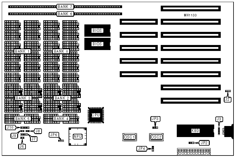
CONNECTIONS | |||
|
Purpose |
Location |
Purpose |
Location |
|
External battery |
J3 |
Turbo LED |
J8 |
|
Turbo switch |
J6 |
Reset switch |
J9 |
|
Speaker |
J7 |
Power LED & keylock |
J10 |
|
USER CONFIGURABLE SETTINGS | |||
|
Function |
Jumper |
Position | |
| » |
Battery type select internal |
J2 |
pins 1 & 2 closed |
|
Battery type select external |
J2 |
pins 2 & 3 closed | |
| » |
Monitor type select monochrome |
JP1 |
pins 1 & 2 closed |
|
Monitor type select color |
JP1 |
pins 2 & 3 closed | |
| » |
CPU speed select OSC1/2 |
JP2 |
pins 1 & 2 closed |
|
CPU speed select OSC2/2 |
JP2 |
pins 2 & 3 closed | |
| » |
Pipeline mode enabled |
JP3 |
pins 1 & 2 closed |
|
Pipeline mode disabled |
JP3 |
pins 2 & 3 closed | |
| » |
Power supply type select AT |
JP4 |
pins 1 & 2 closed |
|
Power supply type select XT |
JP4 |
pins 2 & 3 closed | |
|
Note:Jumper JP1 may not be present on all board revisions. | |||
|
DRAM CONFIGURATION | |||||||||
|
Size |
Bank 0 |
Bank 1 |
Bank 2 |
Bank 3 |
Bank 4 |
Bank 5 |
Bank 6 |
Bank 7 |
Intrlve |
|
640KB 1 |
41256 |
4164 |
41256 |
4164 |
41256 |
4164 |
NONE |
NONE |
NONE |
|
640KB 1 |
NONE |
4164 |
514256 |
NONE |
41256 |
NONE |
NONE |
NONE |
NONE |
|
1MB 1 |
41256 |
41256 |
41256 |
41256 |
41256 |
41256 |
NONE |
NONE |
2-Way |
|
1MB 1 |
NONE |
NONE |
514256 |
514256 |
41256 |
41256 |
NONE |
NONE |
2-Way |
|
1MB 2 |
NONE |
NONE |
NONE |
NONE |
NONE |
NONE |
256K x 9 |
256K x 9 |
2-Way |
|
1.5MB 1 |
41256 |
41256 |
41256 |
41256 |
41256 |
41256 |
256K x 9 |
NONE |
2-Way |
|
1.5MB 1 |
NONE |
NONE |
514256 |
514256 |
41256 |
41256 |
256K x 9 |
NONE |
2-Way |
|
2MB 1 |
41256 |
41256 |
41256 |
41256 |
41256 |
41256 |
256K x 9 |
NONE |
4-Way |
|
2MB 1 |
NONE |
NONE |
514256 |
514256 |
41256 |
41256 |
256K x 9 |
256K x 9 |
4-Way |
|
2MB 1 |
411000 |
NONE |
411000 |
NONE |
411000 |
NONE |
NONE |
NONE |
NONE |
|
2MB 2 |
NONE |
NONE |
NONE |
NONE |
NONE |
NONE |
1M x 9 |
NONE |
NONE |
|
3MB 1 |
41256 |
41256 |
41256 |
41256 |
41256 |
41256 |
1M x 9 |
NONE |
2-Way |
|
3MB 1 |
NONE |
NONE |
514256 |
514256 |
41256 |
41256 |
1M x 9 |
NONE |
2-Way |
|
4MB 1 |
411000 |
411000 |
411000 |
411000 |
411000 |
411000 |
NONE |
NONE |
2-Way |
|
4MB 2 |
NONE |
NONE |
NONE |
NONE |
NONE |
NONE |
1M x 9 |
1M x 9 |
2-Way |
|
5MB 1 |
41256 |
41256 |
41256 |
41256 |
41256 |
41256 |
1M x 9 |
1M x 9 |
2-Way |
|
5MB 1 |
NONE |
NONE |
514256 |
514256 |
41256 |
41256 |
1M x 9 |
1M x 9 |
2-Way |
|
6MB 1 |
411000 |
411000 |
411000 |
411000 |
411000 |
411000 |
1M x 9 |
NONE |
4-Way |
|
8MB 1 |
411000 |
411000 |
411000 |
411000 |
411000 |
411000 |
1M x 9 |
1M x 9 |
4-Way |
|
Notes:Bank 0 and Bank 1 use 12 of the specified DIPP DRAM per bank. Bank 2 and Bank 3 use 4 of the specified DIPP DRAM per bank. Bank 4 and Bank 5 use 2 of the specified DIPP DRAM per bank. Bank 6 and Bank 7 use 2 of the specified SIPP DRAM per bank. Memory interleaving (Intrlve) is automatically configured and is not alterable. Note 1 :On Jumper JP6, pins 1 & 2 should be in the closed position.Note 2 :On Jumper JP6, pins 2 & 3 should be in the closed position. | |||||||||