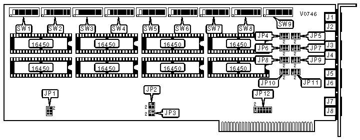
QUATECH, INC.
MS-100, MS-100S
|
Card Type |
Serial interface |
|
Chipset Controller |
Unidentified |
|
I/O Options |
Serial ports (8) |
|
Maximum Dram |
N/A |

|
CONNECTIONS | |||
|
Purpose |
Location |
Purpose |
Location |
|
Serial port 1 |
J1 |
Serial port 5 |
J5 |
|
Serial port 2 |
J2 |
Serial port 6 |
J6 |
|
Serial port 3 |
J3 |
Serial port 7 |
J7 |
|
Serial port 4 |
J4 |
Serial port 8 |
J8 |
|
INTERRUPT SELECTION | |
|
IRQ |
JP12 |
|
2 |
Pins 1 & 2 closed |
|
3 |
Pins 3 & 4 closed |
|
4 |
Pins 5 & 6 closed |
|
5 |
Pins 7 & 8 closed |
|
6 |
Pins 9 & 10 closed |
|
7 |
Pins 11 & 12 closed |
|
COMPATIBILITY MODE SELECTION | |||
|
Port 1 |
Port 2 |
JP2 |
JP3 |
|
COMn: compatible |
COMn: compatible |
Closed |
Closed |
|
COMn: compatible |
Proprietary mode |
Closed |
Open |
|
Proprietary mode |
COMn: compatible |
Open |
Closed |
|
Proprietary mode |
Proprietary mode |
Open |
Open |
|
SERIAL PORT 1 CONFIGURATION | |
|
Setting |
SW1/1 |
|
Enabled |
On |
|
Disabled |
Off |
|
Notes: For serial ports 2 through 8, use SW2/1 through SW8/1, respectively. | |
|
SERIAL PORT 1 ADDRESS SELECT | |||||||
|
Address |
SW1/2 |
SW1/3 |
SW1/4 |
SW1/5 |
SW1/6 |
SW1/7 |
SW1/8 |
|
000h |
On |
On |
On |
On |
On |
On |
On |
|
008h |
On |
On |
On |
On |
On |
On |
Off |
|
010h |
On |
On |
On |
On |
On |
Off |
On |
|
018h |
On |
On |
On |
On |
On |
Off |
Off |
|
220h (COM7:) |
Off |
On |
On |
On |
Off |
On |
On |
|
228h (COM8:) |
Off |
On |
On |
On |
Off |
On |
Off |
|
2E0h (COM6:) |
Off |
On |
Off |
Off |
Off |
On |
On |
|
2E8h (COM4:) |
Off |
On |
Off |
Off |
Off |
On |
Off |
|
2F8h (COM2:) |
Off |
On |
Off |
Off |
Off |
Off |
Off |
|
3E0h (COM5:) |
Off |
Off |
Off |
Off |
Off |
On |
On |
|
3E8h (COM3:) |
Off |
Off |
Off |
Off |
Off |
On |
Off |
|
3F8h (COM1:) |
Off |
Off |
Off |
Off |
Off |
Off |
Off |
|
7E0h |
Off |
Off |
Off |
Off |
Off |
On |
On |
|
7E8h |
Off |
Off |
Off |
Off |
Off |
On |
Off |
|
7F0h |
Off |
Off |
Off |
Off |
Off |
Off |
On |
|
7F8h |
Off |
Off |
Off |
Off |
Off |
Off |
Off |
|
Notes: For serial ports 2 through 8, use SW2 through SW8, respectively. A total of 127 memory base address settings are available. The switches are a binary representation of the decimal addresses. Switch 8 is the Least Significant Bit and switch 2 is the Most Significant Bit. The switches have the following decimal values: switch 8=1, 7=2, 6=4, 5=8, 4=16, 3=32, 2=64. Turn off the switches and add the off switches to obtain the correct memory base address. (On=0, Off=1) | |||||||
|
STATUS REGISTER ADDRESS SELECT | |||||||
|
Address |
SW9/2 |
SW9/3 |
SW9/4 |
SW9/5 |
SW9/6 |
SW9/7 |
SW9/8 |
|
000h |
On |
On |
On |
On |
On |
On |
On |
|
008h |
On |
On |
On |
On |
On |
On |
Off |
|
010h |
On |
On |
On |
On |
On |
Off |
On |
|
018h |
On |
On |
On |
On |
On |
Off |
Off |
|
7E0h |
Off |
Off |
Off |
Off |
Off |
On |
On |
|
7E8h |
Off |
Off |
Off |
Off |
Off |
On |
Off |
|
7F0h |
Off |
Off |
Off |
Off |
Off |
Off |
On |
|
7F8h |
Off |
Off |
Off |
Off |
Off |
Off |
Off |
|
A total of 127 memory base address settings are available. The switches are a binary representation of the decimal addresses. Switch 8 is the Least Significant Bit and switch 2 is the Most Significant Bit. The switches have the following decimal values: switch 8=1, 7=2, 6=4, 5=8, 4=16, 3=32, 2=64. Turn off the switches and add the off switches to obtain the correct memory base address. (On=0, Off=1) | |||||||
|
STATUS REGISTER CONFIGURATION | |
|
Setting |
SW9/1 |
|
Enabled |
On |
|
Disabled |
Off |
|
INPUT CLOCK DIVISOR SELECT | |||
|
JP1 | |||
|
Diveide by 10 (Default) |
Divide by 5 |
Divide by 2 |
Divide by 1 |
|
|
|
|
|
|
SERIAL PORT 1 DTE/DCE SELECTION | |
|
JP4 | |
|
DTE |
DCE |
|
|
|
|
Note: For ports 2-8, use JP5 through JP11, respectively. | |